When I write code for an embedded microprocessor, I frequently need to use communications protocols that allow the micro to communicate with other chips. Often there are peripherals built in to the micro that will handle the bulk of the work for me, freeing up micro clock cycles and allowing me to write fewer lines of code. Indeed, the bulk of modern microcontroller datasheets is usually devoted to explaining these peripherals. So, if you aren't trying to do anything unusual, your micro may have a peripheral that will do most of the work for you. There might be a pre-existing driver library you can use to drive the peripheral. But, sometimes, you don't have a peripheral, or it won't do just what you need it to do, for one reason or another In that case, or if you just want to learn how the protocols work, you can probably seize control of the GPIO pins and implement the protocol yourself.
That's what I will do, in the example below. I will show you how to implement the SPI (Serial Peripheral Interface) protocol, for communicating with an EEPROM. I've used SPI communication in a number of projects on a number of microcontrollers now. The basics are the same, but there are always issues to resolve. The SPI standard is entertaining keeps you on your toes, precisely because it is so non-standard; just about every vendor extends or varies the standard a bit.
The basics of SPI are pretty simple. There are four signals: chip select, clock, incoming data, and outgoing data. The protocol is asymmetrical; the microcontroller is usually the master, and other chips on the board are slaves -- although it would be possible for the micro to act as a slave, too. The asymmetry is because the master drives the chip select and clock. In a basic SPI setup, the slaves don't drive these signals; the slave only drives one data line. I'll be showing you how to implement the master's side of the conversation.
Chip select, sometimes known as slave select from the perspective of the slave chip, is a signal from the master to the slave chip. This signal cues the slave chip, informing the chip that it is now "on stage," ready for its close-up, and it should get ready to communicate. Whether the chip select is active high, or active low, varies. Chip select can sometimes be used for some extra signalling, but in the basic use case the micro set the chip select to the logically active state, then after a short delay, starts the clock, runs the clock for a while as it sets and reads the data signals, stops the clock, waits a bit, and turns off the chip select.
Here's a picture showing the relationship between clock and chip select, as generated by my code. Note that I have offset the two signals slightly in the vertical direction, so that it is easier to see them:

The clock signal is usually simple. The only common question is whether the clock is high when idle, or low when idle. Clock speeds can vary widely. Speeds of 2 to 10 MHz are common. Often you can clock a part much slower, though. CMOS parts can be clocked at an arbitrarily slow speed; you can even stop the clock in the middle of a transfer, and it will wait patiently.
What is less simple is the number of clocks used in a transaction. That can become very complex. Some parts use consistent transfer lengths, where for each transaction, they expect the same number of clock cycles. Other parts might use different numbers of clock cycles for different types of commands.
From the perspective of the slave, the incoming data arrives on a pin that is often known, from the perspective of the microcontroller, as MOSI (master out, slave in). This is again a simple digital signal, but the exact way it is interpreted can vary. Essentially, one of the possible clock transitions tells the slave to read the data. For example, if the clock normally idles low, a rising clock edge might signal the slave to read the data. For reliability, it is very important that the master and slave are in agreement about which edge triggers the read. Above all, you want to avoid the case where the slave tries to read the incoming data line on the wrong edge, the edge when the master is allowed to change it. If that happens, communication might seem to work, but it works only accidentally, because the slave just happens to catch the data line slightly after it has changed, and it may fail when the hardware parameters change slightly, such as when running at a higher temperature.
Let me be as clear as I can: when implementing communication using SPI, be certain you are very clear about the idle state of the clock line, and which clock transition will trigger the slave to read the data line. Then, make sure you only change the data line on the opposite transition.
Terminology surrounding SPI transactions can be very confusing. According to Wikipedia and Byte Paradigm, polarity zero means the clock is zero (low) when inactive; polarity one means the clock is one (high) when inactive.
Phase zero means the slave reads the data on the leading edge, and the master can change the value on the trailing edge, while phase one means the slave reads the data line on the rising edge, and the master changes the data line on the falling edge).But some Atmel documentation (like this application note PDF file) uses the opposite meaning for "phase," where phase one means the slave reads data on the leading edge.
Because of this confusion, in my view it is best not to specify a SPI implementation by specifying "polarity" and "phase." So what would be clearer?
Aardvark tools use the terms "rising/falling" or "falling/rising" to describe the clock behavior, and "sample/setup" or "setup/sample" to indicate the sampling behaviors. I find this to be less ambiguous. If the clock is "rising/falling," it means that the clock is low when idle, and rises and then falls for each pulse. If the "sample" comes first, it means that the slave should read the data line on the leading edge, and if the "setup" comes first, it means that the slave should read the data on the trailing edge.
Here's a picture of my clock signal along with my MOSI (master out, slave in) signal. This SPI communication variant is "rising/falling" and "sample/setup." In order to allow the slave to read a valid bit on the leading clock edge, my code sets the MOSI line to its initial state before the rising edge of the first clock pulse. Again, I have offset the signals slightly in the vertical direction, so that it is easier to see them:

In the screen shot above, the master is sending nine bits: 100110000. Each bit is sampled on the rising clock edge. On the first rising clock edge, the MOSI line (in blue) is high. On the second rising clock edge, the MOSI line is low.
From the perspective of the slave, the outgoing data is sent on a pin that is often known as MISO (master in, slave out). This works in a similar way as the incoming data, except that the slave asserts the line.
When the master sends data to the slave, the master turns on the chip select (whether that means setting it low, or setting it high), changes the MOSI line and clock as needed, and then turns off the chip select.
When the master receives data from the slave, the behavior is slightly more confusing. To get data from the slave, the master has to generate clock cycles. This means that it is also sending something, depending on how it has set the MOSI line. During the read operation, what it is sending may consist of "I don't care" bits that the slave will not read. Receiving data can sometimes require one transaction to prepare the slave for the read operation, and then another to "clock in" the data. Sometimes a receive operation may be done as one transaction, but with two parts: the master sends a few bits indicating a read command, and then continues to send clock cycles while reading the slave's data line. Sometimes there are dummy bits or extra clock cycles in between the parts of this transaction.
Here's a picture that shows a read operation. I'm showing clock and MISO (mmmm... miso!) This shows a long transaction where the master sends a request (the MOSI line is not shown in this picture) and then continues to generate clock pulses while the slave toggles the MISO line to provide the requested data.

Now let's look at my hardware and software. I wrote some code to allow an Arduino Uno to communicate with a serial EEPROM chip. The chip in question is a M93C46 part. This is a 1Kb (one kilobit, or 1024 bits) chip. The parts are widely available from different vendors. I have a few different through-hole versions that I got from various eBay sellers; in testing them, they all worked fine. The datasheet I used for reference is from the ST Microelectronics version of the part.
These parts all seem to have similar pinouts. Pin 1 is the chip select, called slave select in the STM documentation. Pin 2 is the clock. Pins 3 and 4 are data pins. On the other side of the chip, there is a pin for +5V or +3.3V, a pin for ground, an unused pin presumably used by the manufacturer for testing, and a pin identified as ORG (organization), which determines whether the data on the chip is organized into 64 16-bit words, or 128 8-bit bytes.
There are other versions of this chip; the 1Kb is only one version. The command set differs slightly between sizes, but it should be pretty easy to adapt my example to a different-sized part. A full driver would be configurable to handle different memory sizes. It would not be hard to implement that, but for this example I am keeping things simple.
Here's my simple circuit, on a prototype shield mounted to an Arduino Uno:
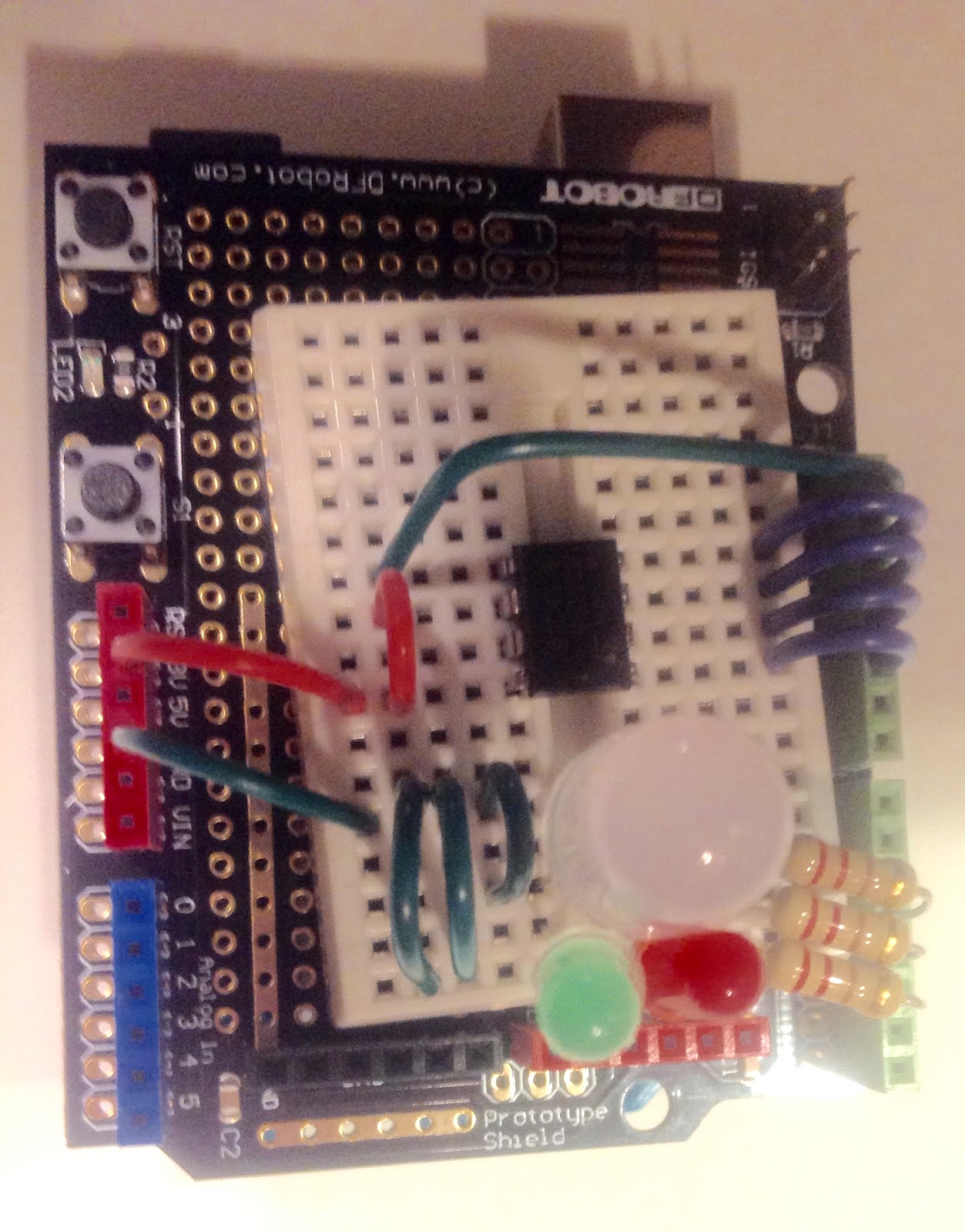
Here's a simple schematic showing the Arduino pins connected to the EEPROM chip:

I'm not much of an electrical engineer, but that should convey that pin 1, usually marked with a little dot or tab on the chip, is on the lower right. We count pins counter-clockwise around the chip. So pin 5 goes to ground (I used the ground next to the data pins; that is the green wire going across the board). Make sure you are careful to connect the right pins to power and ground, or you can let the magic smoke one of these little EEPROM chips, and maybe disable your Arduino board, too, perhaps permanently (you'll never guess how I know this!)
I also have three LEDs connected to three more pins, connected through 220 ohm resistors, with the negative side of the LEDs going to a ground pin on the left side of the prototype board. Those are not required; they are there solely to create a simple busy/pass/fail display. You can use the serial monitor, if the Arduino is attached to your computer, or whatever other debugging method is your favorite.
I have done this kind of debugging with elaborate, expensive scopes that have many inputs and will decode SPI at full speed. That is very nice, but you don't necessarily need all for a simple project like this. I got this project working using a Rigol two-channel scope. I was not able to capture a trace of all our lines at once using this scope, but I didn't need to. With two channels, I could confirm that the chip select and clock were changing correctly with respect to each other. Then I could look at the MOSI along with the clock and verify that the data was changing on the expected clock transition. Then I could look at the MISO along with the clock to verify the bits the Arduino was getting back from the serial EEPROM chip. Here's my modest setup, using a separate breadboard rather than a shield:

Here's a view of a SPI conversation with the EEPROM chip: a write operation, followed by a read operation to verify that I can get back what I just wrote. This shows clock and MOSI, so we don't see the slave's response, but you can see that the second burst has a number of clock cycles where the master is not changing the data line. Those are "don't care" cycles where the master is listening to what the slave is saying. Note also that I am running this conversation at a very slow clock speed; each transition is 1 millisecond apart, which means that my clock is running at 500 Hertz (not MHz or even KHz). I could certainly run it faster, but this makes it easy to see what is happening, if I toggle an LED along with the chip select to show me when the master is busy.

Now, here's some code.
You don't have to use these pins, but these are the ones I used.
#define SLAVESELECT 10 /* SS   */
#define SPICLOCK    11 /* SCK  */
#define DATAOUT     12 /* MOSI */
#define DATAIN      13 /* MISO */
Here's a "template" 32-bit word that holds a 16-bit write command.
#define CMD_16_WRITE ( 5UL  << 22 )
#define CMD_16_WRITE_NUM_BITS ( 25 )
This defines a 25-bit command. There is a start bit, a 2-bit opcode, a six-bit address (for selecting addresses 0 through 63), and 16 data bits.
To use this template to assemble a write command, there's a little helper function:
uint32_t assemble_CMD_16_WRITE( uint8_t addr, uint16_t val )
{
    return ( uint32_t )CMD_16_WRITE   |
           ( ( uint32_t )addr << 16 ) |
             ( uint32_t )val;
}
Now we need a function that will send that command. First, let's start with a function that will send out a sequence of bits, without worrying about the chip select and final state of the clock.
void write_bit_series( uint32_t bits, uint8_t num_bits_to_send )
{
    uint8_t num_bits_sent;

    for ( num_bits_sent = 0; num_bits_sent < num_bits_to_send;
          num_bits_sent += 1 )
    {
        digitalWrite( SPICLOCK, LOW );
        digitalWrite( DATAOUT, bits & ( 1UL <<
            ( num_bits_to_send - num_bits_sent - 1 ) ) ? HIGH : LOW );
        delay( INTER_CLOCK_TRANSITION_DELAY_MSEC );
        digitalWrite( SPICLOCK, HIGH );
        delay( INTER_CLOCK_TRANSITION_DELAY_MSEC );

    }

}
This maps the bits to the DATAOUT (or MISO) line. We change the data line on the falling edge of the clock. We aren't using a peripheral to handle the SPI data; we just "bit bang" the outputs using a fixed delay.
Here's a function that will send a command that is passed to it. It works for write commands:
void write_cmd( uint32_t bits, uint8_t num_bits_to_send )
{
    digitalWrite( SLAVESELECT, HIGH );
    delay ( SLAVE_SEL_DELAY_PRE_CLOCK_MSEC );

    write_bit_series( bits, num_bits_to_send );

    /*
        Leave the data and clock lines low after the last bit sent
     */
    digitalWrite( DATAOUT, LOW );
    digitalWrite( SPICLOCK, LOW );

    delay ( SLAVE_SEL_DELAY_POST_CLOCK_MSEC );
    digitalWrite( SLAVESELECT, LOW );

}
That's really all you need to send out a command. For example, you could send a write command like this:
write_cmd( assemble_CMD_16_WRITE( addr, write_val ), CMD_16_WRITE_NUM_BITS );
Note that before you can write successfully, you have to set the write enable. My code shows how to do that. Basically, you just define another command:
#define CMD_16_WEN   ( 19UL <<  4 )
#define CMD_16_WEN_NUM_BITS   (  9 )

write_cmd( ( uint16_t )CMD_16_WEN, CMD_16_WEN_NUM_BITS );
This EEPROM chip will erase each byte or word as part of a write operation, so you don't need to perform a separate erase. That may not be true of all EEPROM chips.
To read the data back, we need a slightly more complex procedure. Our read command uses the write_bit_series function to send out the first part of the read command, then starts clocking out "don't care" bits and reading the value of the MOSI line:
uint16_t read_16( uint8_t addr )
{
    uint8_t num_bits_to_read = 16;
    uint16_t in_bits = 0;
    uint32_t out_bits = assemble_CMD_16_READ( addr );

    digitalWrite( SLAVESELECT, HIGH );
    delay ( SLAVE_SEL_DELAY_PRE_CLOCK_MSEC );

    /*
        Write out the read command and address
    */
    write_bit_series( out_bits, CMD_16_READ_NUM_BITS );

    /*
        Insert an extra clock to handle the incoming dummy zero bit
    */
    digitalWrite( DATAOUT, LOW );

    digitalWrite( SPICLOCK, LOW );
    delay( 1 );

    digitalWrite( SPICLOCK, HIGH );
    delay( 1 );

    /*
        Now read 16 bits by clocking. Leave the outgoing data line low.
        The incoming data line should change on the rising edge of the
        clock, so read it on the falling edge.
    */
    for ( ; num_bits_to_read > 0; num_bits_to_read -= 1 )
    {
        digitalWrite( SPICLOCK, LOW );
        uint16_t in_bit = ( ( HIGH == digitalRead( DATAIN ) ) ? 1UL : 0UL );
        in_bits |= ( in_bit << ( num_bits_to_read - 1 ) );
        delay( INTER_CLOCK_TRANSITION_DELAY_MSEC );

        digitalWrite( SPICLOCK, HIGH );
        delay( INTER_CLOCK_TRANSITION_DELAY_MSEC );
    }

    /*
        Leave the data and clock lines low after the last bit sent
     */
    digitalWrite( DATAOUT, LOW );
    digitalWrite( SPICLOCK, LOW );

    delay ( SLAVE_SEL_DELAY_POST_CLOCK_MSEC );
    digitalWrite( SLAVESELECT, LOW );

    return in_bits;

}
And that's the basics. To test this, I put an EEPROM chip on a breadboard and just wired up the pins as specified in the code. Check your datasheet to determine if you can power the part with 5V or 3V. The chips I got seem to work fine with either, although if you are testing with a scope, you might want to use 5V so that the data out you get back from the chip has the same level as the 5V Arduino outputs.
You can find the full sketch on GitHub here.
Good luck, and if you found this useful, let me know by posting a comment. Comments are moderated, so they will not show up immediately, but I will post all (non-abusive, non-spam) comments. Thanks for reading!


